|

|
|
|
Recent Publications |
Department of Electronic and Electrical Engineering Office: Roberts 1119 Tel: +44 (0)20 7679 3128 Email: o.mitrofanov at ucl.ac.uk |
Rubrene Crystals |
Role of synthesis for oxygen defect incorporation in crystalline rubreneApplied Physics Letters 91, 212106 (2007) PDF
Oleg Mitrofanov, |
|
Understanding of the impact of molecular structure on charge transport in organic molecular crystals and thin films is the basis for control and manipulation of their electronic properties. It is critical however to recognize that morphology and presence of defects, either structural or chemical, affect the charge transport in organic solids as much as the molecular structure. In crystalline rubrene, the material that exhibits one of the highest charge carrier mobilities among acenes, incorporation of the oxygen-related defect can significantly increase electrical conductivity. In this work, a photoluminescence signature of the defect is used to investigate the defect formation mechanisms. Our experimental results show that impurity incorporation can occur during the growth, if residual oxygen is present in the furnace, as well as after the crystal growth in a normal environment. The post growth oxidation appears to be driven by the presence of structural disorder in rubrene crystals in a form of vacancies or grain boundaries. This correlation is likely caused by the structure of the impurity, a rubrene peroxide molecule. To accommodate a rubrene peroxide molecule in rubrene crystal lattice a vacancy is required at a neighbouring site. The lattice therefore suppresses the postgrowth rubrene-oxygen reaction, making high-quality rubrene crystals less susceptible to the oxidation process. These findings are central in understanding of the material quality impact on electronic and optical properties of rubrene crystals. |

Packing of rubrene molecules (Carbon atoms in the tertacene backbone are coloured yellow for clarity). |
Oxygen-Related Bandgap State in Single Crystal RubrenePhysical Review Letters 97, 166601 (2006) PDF
O. Mitrofanov
|
|
Using photoluminescence spectroscopy with single- and two-photon excitation and charge transport analysis this work shows that large variations of the carrier density in rubrene are caused by an oxygen-related impurity, which acts as an acceptor state. Among several photoluminescence bands corresponding to different electronic and vibronic transitions in rubrene crystals, we identified a band emitted due to the presence of an oxygen-related impurity. Our experiments show direct correlations of this O-band, sometimes mistakenly regarded as the photoluminescence signature of pure crystalline rubrene, and the defect. This impurity however plays an important role in charge transport in rubrene crystals. A large increase in electrical conductivity of oxidized crystals and the well-defined spectroscopic signature of the defect indicate that the impurity forms a bandgap state near the valence band. Control of the impurity presence therefore allows modifying the material conductivity. |

PL characteristics of rubrene crystals in the direction normal to ab-surface: band III is the dominant feature for pure crystals, while band O around 645 nm (1.92 eV) indicates crystal oxidation |
Terahertz Waveguides |
Low-loss modes in hollow metallic terahertz waveguides with dielectric coatingsApplied Physics Letters 93, 181104 (2008) PDF
Bradley Bowden and James A. Harrington (Rutgers U.) |
|
Silver/polystyrene-coated hollow glass waveguides for the transmission of terahertz radiationOptics Letters 32, 2945-2947 (2007) PDF
Bradley Bowden and James A. Harrington (Rutgers U.) |
|
Existing waveguiding solutions suffer from high loss at THz frequencies either due to material absorption in dielectric waveguides or due to finite conductivity in metallic waveguides. These losses are substantially reduced in hollow metallic waveguides with a thin dielectric coating. This work describes low-loss waveguides for THz waves (1-3 THz) developed in Rutgers University. Cylindrical waveguides are designed to support the HE11 mode important for many practical applications. Characterization of the waveguides shows good mode quality with the total loss below 1 dB/m at 2.5 THz. The low loss is achieved by improving reflectivity of the waveguide walls by means of a thin dielectric layer on the inner metallic surface. These low-loss THz waveguides open possibilities for applications in communications and sensing. |

Transverse and Hybrid modes in hollow THz waveguides |
Terahertz Near-Field Microscopy |
Waveguide Mode Imaging and Dispersion Analysis with Terahertz near-field microscopyApplied Physics Letters 94, 171104 (2009) PDF
Oleg Mitrofanov, Thomas Tan |
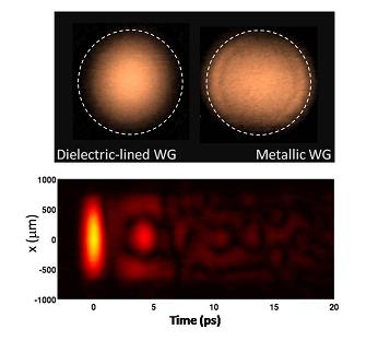
Main modes in hollow metallic waveguides with and without the dielectric coating (top). Space-time map of a THz pulse propagating as two modes: HE11 and HE12 (bottom). |
Terahertz near-field electro-optic probe based on a microresonatorApplied Physics Letters 88, 091118 (2006), PDFOleg Mitrofanov
|
|
Research in the area of THz devices demands experimental characterization tools. This work describes a local miniature probe for measurements of high-frequency electric fields through the linear electro-optic effect. To reduce the probe size a microresonator is employed instead of a bulk electro-optic crystal. The microresonator structure defines the detection region of only 2 micrometers and enhances the probe sensitivity within the detection bandwidth of 1THz. The microresonator probe can be used for THz near-field imaging and spectroscopy as well as for non-invasive electro-optic sampling of high-speed integrated circuits. |

Fibre-coupled EO probe with a GaAs crystal |
University College London - Gower Street - London - WC1E 6BT - ![]() +44 (0)20 7679 2000 - Copyright © 1999-2005 UCL
+44 (0)20 7679 2000 - Copyright © 1999-2005 UCL