|

|
|
|
THz near-field microscopy applications in device research |
Ultrafast Laser Laboratory Department of Electronic and Electrical Engineering |
|
The technology of THz near-field imaging experienced significant advances since the first demonstration in the late 1990's: novel near-field probes have been developed and various applications have been demonstrated [1]. THz near-field microscopy is now making an impact on the development of THz technology. High spatial resolution and the possibility of time-domain analysis make this method invaluable for research on THz devices. The near-field method helps understand the underpinning device physics by visualising THz waves with a sub-wavelength spatial resolution, greatly surpassing the diffraction limit. It allows measurements of device characteristics that are difficult or impossible to assess with far-field methods. We recently applied the near-field microscopy technique for characterisation of THz waveguides. The multimode nature of most THz waveguides makes the time-domain spectroscopy analysis difficult in application to waveguides due to mode interference. The near-field microscopy solves the multimode problem by providing space-time maps of the propagating wave in which the waveguide modes can be distinguished [2]. The visualization of the propagating THz waves showed for the first time the mode structure in the dielectric-lined hollow metallic waveguides. It also showed the impact of the spatial mode profile on the loss and dispersion characteristics. We also applied the near-field method for imaging of THz surface plasmon waves. This type of waves is in the core of many interesting phenomena, such as the extraordinary transmission of sub-wavelength hole arrays and the negative value of the refractive index in metamaterials. The surface waves provide a useful possibility to guide and confine THz waves near metallic surfaces without radiation. The non-radiative nature prevents observation of the surface waves by far-field methods. They however can be detected locally by the near-field probe and their role in operation of THz devices can be studied with the near-field microscope [3]. |
|
NEAR-FIELD MICROSCOPY SYSTEM Most THz near-field probes that have been developed recently can be used for device research. Each probe type has specific advantages: electro-optic probes provide a remarkable possibility to detect individual components of the electric field; scattering needle probes allow mapping of the THz field with an unprecedented spatial resolution. In our studies, we use an integrated sub-wavelength aperture probes, which provide excellent sensitivity and a wavelength-independent spatial resolution better than 10 microns [4]. This probe has a well-understood frequency response, covering a broad band of frequencies from about 0.2 THz to 3 THz [4]. The near-field probe consists of a GaAs-based photoconductive antenna detector and a small aperture in a metallic screen (Fig. 1). A short distance between the aperture and the photoconductive antenna allows detecting evanescent waves that couple through the aperture and therefore improve the detector sensitivity. For near-field imaging and spectroscopy studies, device samples are placed on a sample platform and illuminated by a THz pulses delivered through a cylindrical waveguide. |
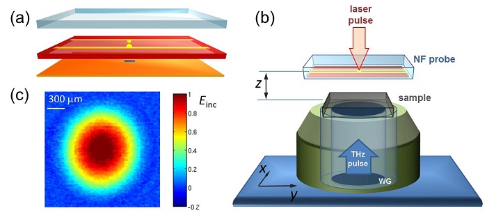
The near-field microscopy system: (a) schematic diagram of the integrated sub-wavelength aperture THz near-field probe; (b) typical arrangement of the near-field probe and the waveguide platform with a sample; (c) distribution of the THz illumination field delivered by a THz waveguide. |
|
MODE IMAGING AND DISPERSION ANALYSIS IN THZ WAVEGUIDES The spatial profile of the dominant mode in a waveguide can give intuitive understanding of the waveguide loss and dispersion characteristics. Experimental studies of the mode profile require the near-field imaging of the waveguide output. In most THz waveguides, the problem of mode characterization however becomes difficult due to mode interference. The time-resolved capability of pulsed THz spectroscopy systems combined with near-field imaging solves the multimode problem by providing space-time maps of the propagating wave at the waveguide output. The time-resolved imaging allows distinguishing the waveguide normal modes and mapping their spatial profiles because the modes separate in time as they travel through the waveguide. This approach avoids the problem of mode interference occurring in the frequency domain. The spatial resolution of the probe also allows measurements of dispersion and losses for individual modes by positioning the probe in a location where the mode of interest has high amplitude whereas other modes have minimal amplitudes. The near-field spectroscopy system provided first experimental measurements of dispersion for main modes in the dielectric-lined hollow cylindrical metallic waveguide (Fig. 2) [5]. In this waveguide, the mode profile explains very low loss (1 dB/m) and relatively low dispersion (6 ps/THz/m) [6]. |

Mode mapping in THz wavesguides: (a) time-resolved near-field spatial maps showing the normal modes of the dielectric-lined cylindrical metallic waveguide; (b) space-time maps at the output of a 133.5 mm long waveguide for three different coupling configurations [5]. |
|
SURFACE PLASMON WAVE IMAGING It was recently discovered that surface plasmon waves can be detected with the integrated aperture probe [3]. This result is not obvious because the detector antenna in the probe is orthogonal to the polarization of the field. Nevertheless, the surface nature of plasmon waves allows them to couple through the probe aperture and to induce a current in the photoconductive antenna detector. This probe was employed for mapping a previously undetected phenomenon, a surface wave formed on a metallic surface by a tightly focused THz beam [3]. The near-field probe can be also applied for studies of surface plasmon resonances in THz devices, such as a THz antenna [7]. Figure 3 shows formation of a standing resonant wave in a bow-tie antenna illuminated by a THz pulse. Transient distributions of the field can be detected by the near-field probe as well. Such images provide an insight into the physics of the antenna response. Our experimental investigations allowed us to deduce the response characteristics of the integrated sub-wavelength aperture probe to the surface plasmon wave (polarized perpendicular to the aperture place): the probe detects a spatial derivative of the surface plasmon field, rather than the field itself [3], [7]. The understanding of the coupling mechanisms now provides a complete framework for analysis and interpretation of images in near-field microscopy. |
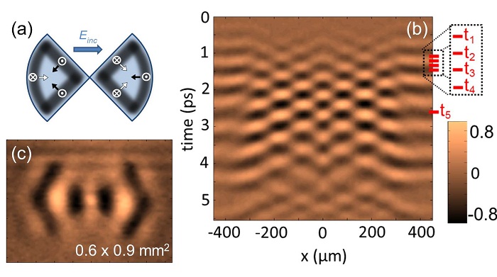
THz surface plasmon waves formed on a bow-tie antenna: (a) schematic diagram of the bow-tie antenna showing the surface waves generated by the incident THz pulse; (b) a space-time map measured along the antenna axis (y=0); (c) THz image of a resonant surface wave formed on the antenna about 2 ps after the arrival of the THz pulse. |
|
FURTHER APPLICATIONS OF NEAR-FIELD MICROSCOPY Examples discussed above outline a potential impact of THz near-field microscopy on THz device research. In these applications, the underlying physics of device operation is uncovered through the detection of non-radiative components of the THz electric field and through local THz spectroscopy. The combination of high-resolution imaging and the time-resolved measurements allows addressing difficult problems in device characterization. Presently, many THz near-field approaches provide sufficient spatial resolution for studies of THz devices. The interaction between a near-field probe and an object however requires further investigations in order to determine which near-field probe is more appropriate for a given application. The interaction can be complex, particularly for near-field probes that contain metallic components. For the integrated sub-wavelength aperture probe, however the coupling mechanism yields a simple analytical relationship between the field near the object and the detected field. The understanding of the coupling mechanism allows further applications of this near-field probe for THz device research. [1] Adam, J. Infrared Milli Terahz Waves (2011). [2] Mitrofanov et al., Appl. Phys. Lett. 94, p. 171104 (2009). [3] Mueckstein and Mitrofanov, Opt. Express 19, 3212-3217 (2011). [4] Mitrofanov, et al., IEEE J. Selected Topics in Quantum Electronics 7, 600-607 (2001). [5] Mitrofanov and Harrington, Optics Express 18, 1898-1903 (2010). [6] Mitrofanov et al., IEEE Trans. on Terahertz Science and Technology 1, (2011) [7] Mueckstein et al., J. Infrared Milli Terahz Waves (2011). |
|
This page contains a summary of the invited talk at IRMMW-THz2011 (Houston, TX USA). |
University College London - Gower Street - London - WC1E 6BT - ![]() +44 (0)20 7679 2000 - Copyright © 1999-2012 UCL
+44 (0)20 7679 2000 - Copyright © 1999-2012 UCL