|

|
|
|
Terahertz Waveguides Research |
Ultrafast Laser Laboratory Department of Electronic and Electrical Engineering |
|
To expand the range of THz applications it is essential to develop waveguides with minimal transmission loss and minimal dispersion. The first requirement is particularly difficult to fulfill because dielectrics and metals exhibit large absorption at THz frequencies. As a result, dielectric guides (such as fibre widely used for optical waves) and hollow metallic waveguides (used for millimeter waves) exhibit transmission losses of ~5-100 dB/m at THz frequencies. What is the best waveguide to transmit THz waves securely and without significant losses? Several waveguide designs, including photonic crystal fibres and parallel-plate metallic guides, are currently investigated in the search for a suitable solution. In 2007, we demonstrated transmission losses below 1 dB/m at THz frequencies in dielectric-lined cylindrical metallic waveguides, where the dominant mode exhibits remarkably low interaction with absorbing waveguide walls (Opt. Lett. 32, 2945 (2007)). Later, we developed technology for visualising THz wave propagation in waveguides. Articles listed below summarise our studies of THz waveguides. | 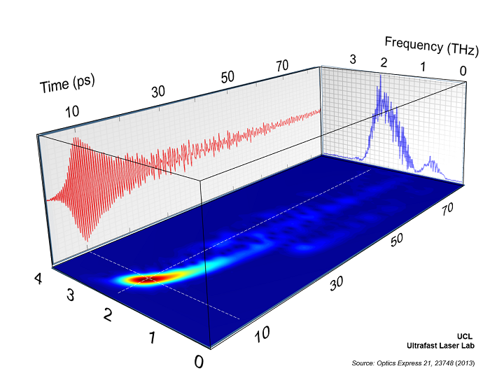 |
|
|
Can broadband THz pulses be transmitted through a waveguide without dispersion and with minimal losses? |
|
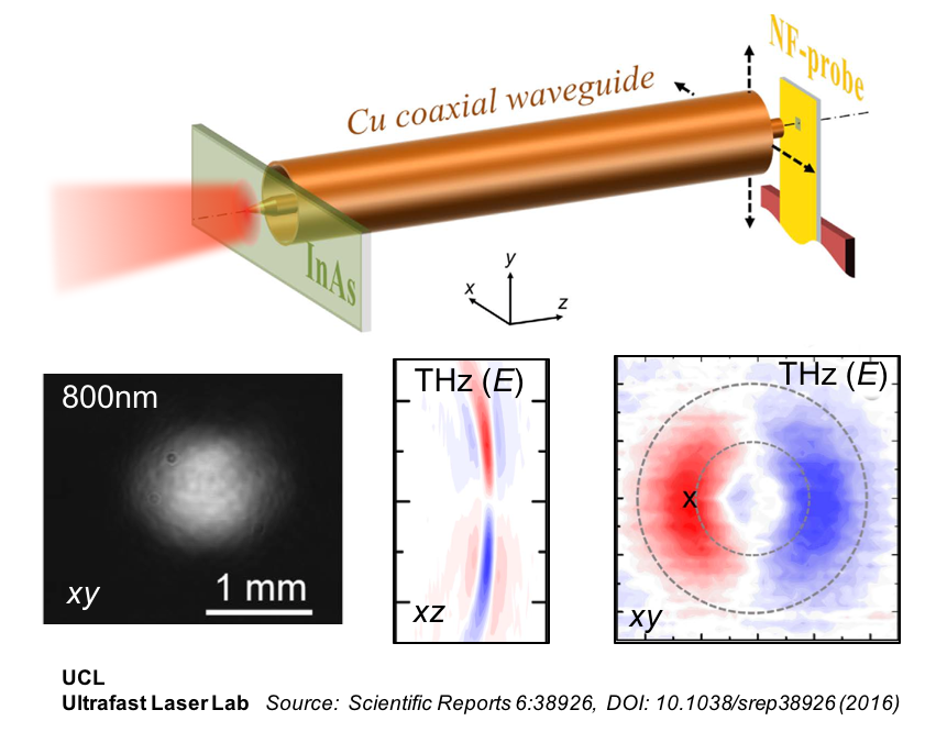
Coaxial waveguides are commonly used for transmission of high-frequency electronic signals, up to the GHz range, because they exhibit minimal or no dispersion, preserving integrity of the signal. Coaxial waveguides are also attractive for transmission of broadband THz pulses, however practical implementations encounter a range of technical problems, including the coupling of THz pulses into the waveguides, which we addressed in this research. We proposed and demonstrated a simple method for generation and efficient coupling of broadband THz pulses into THz coaxial waveguides. This article discusses launching of THz pulses into coaxial waveguides using the effect of THz pulse generation at semiconductor surfaces. We found that the radial transient photo-currents produced upon optical excitation of semiconductors radiate THz pulses with the field distribution naturally matching the fundamental TEM mode of the coaxial waveguide. This mode enables propagation of broadband THz pulses in an air-filled coaxial waveguide with no dispersion and small transmission losses. We demonstrate a simple scheme (illustrated in the diagram), where the optical excitation beam of an InAs plate produces a radially-polarised THz wave, which couples into the hollow coaxial THz waveguide. The spatial profile and the polarisation state of the THz pulse can be tailored by the spatial profile of the optical excitation. In our case, the diameter of the optical beam allows us to optimise the spatial profile of the generated THz pulse for efficient waveguide coupling.
Scientific Reports 6, 38926 (2016) Nature linkCopyright 2016Graphics: Illustration of THz pulse generation directly into the coaxial waveguide mode |
|
Split shell design suppresses the cutoff effect in conical metallic waveguides |
|
In collaboration with the University of Utah, we demonstrated focusing of terahertz (THz) waves to subwavelength diameter beams using a split conical waveguide. Such waveguide can be used for practical imaging using THz waves with spatial resolution better than the diffraction limit. Conical waveguides can focus electromagnetic waves, however not for all frequencies. To mitigate this problem, known as the cutoff effect, we designed and investigated a conical tapered waveguide, which consist of two pieces, such that there is an adjustable gap along the waveguide length. Thin sidewalls in the vicinity of the gap prevent energy leakage through the gaps. Such a waveguide focuses THz waves within a wider spectrum without compromising the mode confinement. We experimentally confirmed the focusing properties using our THz near-field imaging system: an incident THz wave is focused to a spot smaller than 100 micrometers (see Graphics). These conical waveguide can be used instead of a lens in THz imaging systems to achieve spatial resolution better than the diffraction limit.
Optics Express 24, 2728 (2016) Optica linkCopyright 2016Graphics: Schematic diagram of the split conical waveguide and the output field profile |
 |
Flexible polystyrene-lined hollow metallic waveguides for the 2.5-5 THz band |
|
In this paper we summarise our investigation of transmission properties of 1 mm-diameter PS-lined waveguides at THz frequencies. We performed broadband (0.5-2.5 THz) cutback loss measurement using our near-field time-domain spectroscopy (TDS) system. This near-field technique mitigates difficulties associated with the variation of the coupling coefficient with frequency and allows us to identify waveguide modes. We verified the near-field transmission loss measurements using single-frequency 2.85 THz quantum cascade laser (QCL). The near-field TDS data show the low-loss transmission band that spans ~2.5 THz, from 2.5 to 5 THz, as confirmed by numerical modeling. Within the transmission band, the waveguides show the attenuation of 4-4.5 dB/m matching the calculated values. These waveguides are suited well for the spectral range of THz QCLs and they can provide a solution for shaping the highly divergent QCL beams. The waveguides are flexible enough to form bends with the radius of curvature as small as 100-150 mm.
Optics Express 21, 23748 (2013) OSA linkCopyright 2013 Optical Society of America. |

|
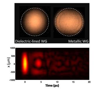
Mode structure and dispersion in dielectric-lined cylindrical metallic THz waveguides |
|
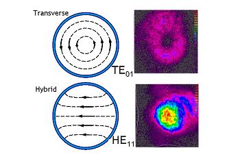
An electro-magnetic wave traveling in a waveguide can be considered as a superposition of basic waveguide modes. Each mode has a unique set of properties including the mode spatial profile, velocity of propagation and attenuation constant. In the dielectric-lined hollow metallic waveguides, the spatial profile is not the same as in the metallic guides without the dielectric coating. The profile shows a very small fraction of the wave energy traveling near the absorbing waveguide walls. As a result the dielectric-lined hollow metallic waveguides exhibit some of the best transmission characteristics among THz waveguides. In this work we investigated the impact of the dielectric layer on the waveguide dispersion. Dispersion characteristics are determined experimentally for the low-loss waveguide modes, the linearly-polarized HE11 mode and the TE01 mode. The results are compared with dispersion in metallic waveguides. Additional dispersion due to the dielectric layer is found to be small for the dominant mode.
Optics Express 18, 1898 (2010) PDF OSA linkThis article may be downloaded for personal use only. Any other use requires prior permission of the author and the Optical Society of America. Copyright 2009 Optical Society of America. |
|
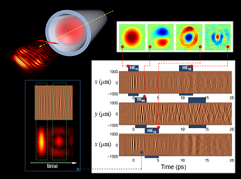
Application of THz near-field microscopy for analysis of modes in THz waveguides |
|
Identification of waveguide modes is essential for studies of the waveguide transmission properties. It helps to optimize the waveguide design and reduce losses, which present a major challenge for THz waveguide research. We applied time-resolved THz near-field microscopy to determine and investigate propagating modes in hollow metallic waveguides. The dominant mode in a hollow metallic waveguide has the electric field terminating abruptly at the waveguide wall, while the dominant mode in a similar waveguide with a thin dielectric coating, has the electric field vanishing near the wall. The change of the mode profile reduces the Ohmic losses substantially in the dielectric-lined waveguides. The near-field images of the waveguide output clearly show the difference in the mode structure (left and right panels). A space-time map (bottom panel) measured with the near-field probe also allows to determine whether higher order modes are present. These modes propagate with lower group velocities and have distinctive electric field spatial patterns.
Applied Physics Letters 94, 171104 (2009) PDF AIP linkThis article may be downloaded for personal use only. Any other use requires prior permission of the author and the American Institute of Physics. Copyright 2009 American Institute of Physics. |
|
Mode-dependent Transmission Losses in Hollow Metallic Waveguides |
|
This work describes cutback loss measurements for two types of metallic waveguides, in which either the TE01 or the HE11 mode has the lowest transmission loss. These waveguides differ only in the thickness of the inner dielectric layer. The classical TE01 mode is the dominant mode for waveguides with ~1-2 micron thick layers (similar to the case of metal-only waveguides). However the HE11 mode becomes the dominant mode if the dielectric layer thickness is increased to ~ 10 microns. The transmission loss in this case falls below 1 dB/m at 2.5 THz. THz waveguides supporting the HE11 mode can become important for practical applications, where the low-loss transmission properties, good mode confinement and efficient coupling to free-space propagating beams is necessary.
Applied Physics Letters 93, 181104 (2008), PDF AIP linkThis article may be downloaded for personal use only. Any other use requires prior permission of the author and the American Institute of Physics. Copyright 2008 American Institute of Physics. |
Transverse and Hybrid modes in hollow THz waveguides |
|
Research was done in collaboration with
|
University College London - Gower Street - London - WC1E 6BT - ![]() +44 (0)20 7679 2000 - Copyright © 1999-2013 UCL
+44 (0)20 7679 2000 - Copyright © 1999-2013 UCL