|

| INFORMATION FOR Prospective Students INFORMATION Home PROJECTS Funded QUICK LINKS Optical Devices
|
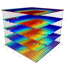
In-Plane Switching (IPS) ModeIn the planar cell, when a voltage is applied the molecules lie perpendicular to the alignment layers. As a result of viewing the molecules end on, the transmittance is very sensitive to viewing angle. The IPS mode is becoming more common in display applications, where interdigitated electrodes promote lateral switching of the director. Since the molecules are viewed side on, the transmittance is much less sensitive to viewing angle.
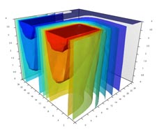
Fig.1: Director stack plot and equi-potential surfaces in an IPS cell
Polarisers are normally crossed and are aligned parallel and perpendicular to the optic axis. Maximum transmittance is achieved when the in-plane electric field reorients the director to lie at 45 degrees to the electrode edge. The cell thickness should be that of a half-wave plate. Fig.1 shows the director field and the equi-potential surface at the end of a IPS electrode. Note the formation of a defect beneath the edge of the shorter electrode.
This page last modified 2 June, 2006 by r.james |