|

| INFORMATION FOR Prospective Students INFORMATION Home PROJECTS Funded QUICK LINKS Optical Devices
|
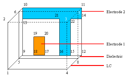
Creating an IPS Structure using TetgenFor in plane switching structures there is an interface at the top and bottom of the structure between the LC and air or glass. Although in the following example this material is neglected, for accurate modelling it is crucial that these layers are included. If the LC boundary is left free, this is equivalent to an interface between LC and a material with dielectric constant of zero! Work is currently underway change this default behaviour to an air-LC interface.
This program visualises results on both irregular and regular 2D and 3D meshes. Director plots can be made across slices, or sampled regularly in 3D space. Iso-surface plots of potential, twist and tilt can be made. Built in Extended optics code, for image plots or viewing angle plots. Free energy calculation, surface and contour plots. Provides a means to rapidly convert results from irregular to regular meshes, as required for most optical calculations To begin with it is necessary to define each node. The definitions can either be placed at the top of the .smesh or .poly file, or defined separately in a .node file, as has been done here.
Each surface is defined in the file below. Multiple surfaces may be defined on each face, but if the .smesh format it used, the created volumes cannot contain holes. The first number on each line gives the number of nodes that defines the surface, which are subsequently listed. The final number is the material number of the surface. The final region section of the file allows a material number to be applied to volumes by defining a point at the centre of the volume, and providing the material number.
This page last modified 2 June, 2006 by r.james |