Most of our research utilises the physics the 2DEG offers. 2DEG can be formed at the interface of the AlGaAs/GaAs semiconductor heterostructure [1]. The desired properties to study the quantum phenomena include control of carrier concentration and high mobility. Usually, semiconductor devices require large amounts of doping to increase the carrier concentration however this leads to more impurities and reduced mobility. On the other hand, higher levels of mobility are usually achieved by decreasing the dopant concentration which reduces mobility. 2DEG offers an optimal situation where both of these values could be large [2].
What does it mean that a layer is two-dimensional? How can we have two-dimensions in the practical world?
Initially, consider an n-doped AlGaAs where the bandgap is increased compared to a GaAs due to the addition of the Al alloy, and the fermi level is a quasi-fermi-level closer to the conduction band due to n-doping. Take the horizontal dimension of the figures as the z-axis.
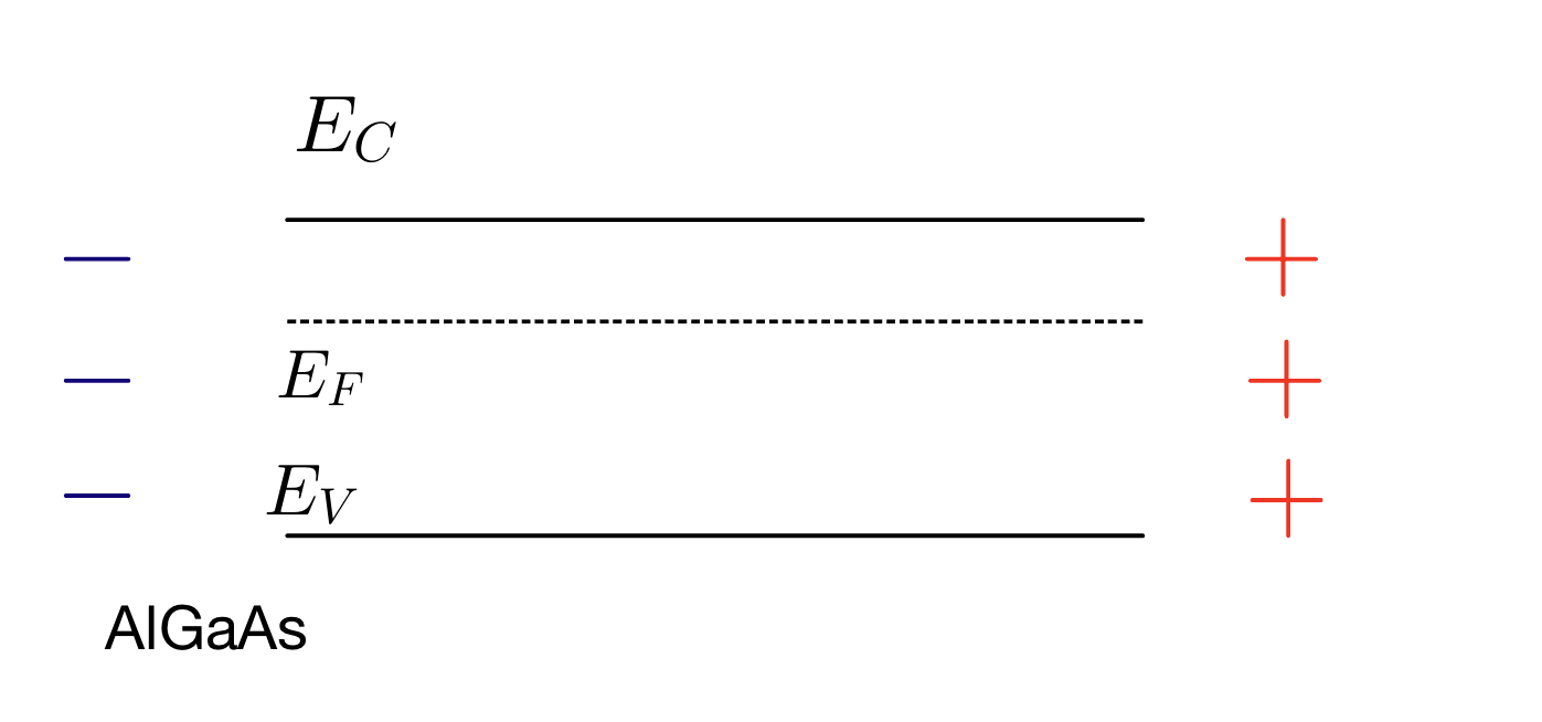
Figure adapted from Ref[3]
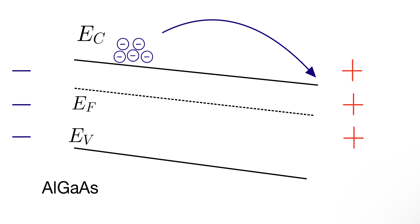
Figure adapted from Ref[3]
The charges above indicate that there is some charge polarisation at the top and bottom of the AlGaAs, in the z-direction. This can be induced during the growth process, which is also equivalent to assuming that there is some voltage being applied around a thin film of AlGaAs [3]. The region with positive charges will bend the bands lower to their side and attract the negative charge carriers.
The attraction of the negative charges to one side leaves behind positive charges on the other, leading to an opposing electric field. Bands will bend to achieve the equilibrium state between two opposing fields with a constant fermi level across the material. The bending (curvature) is induced by the distribution of the charge densities [4].
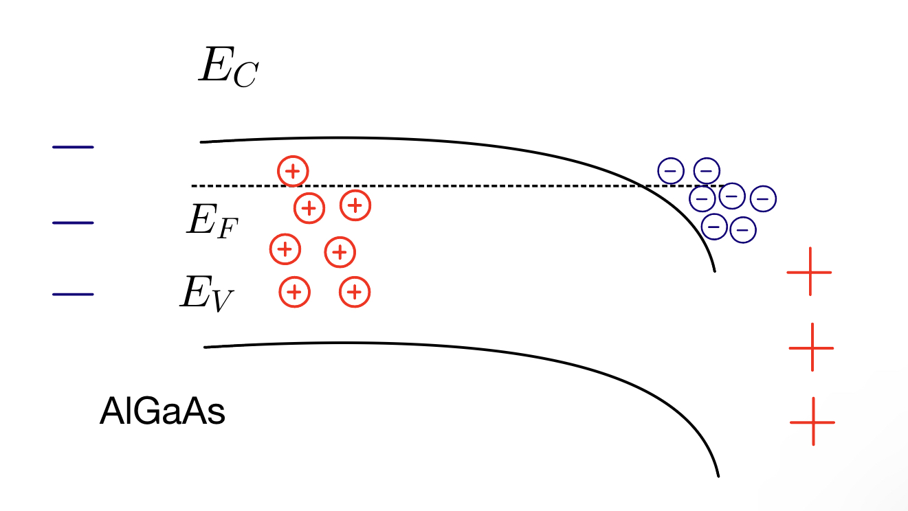
Figure adapted from Ref[3]
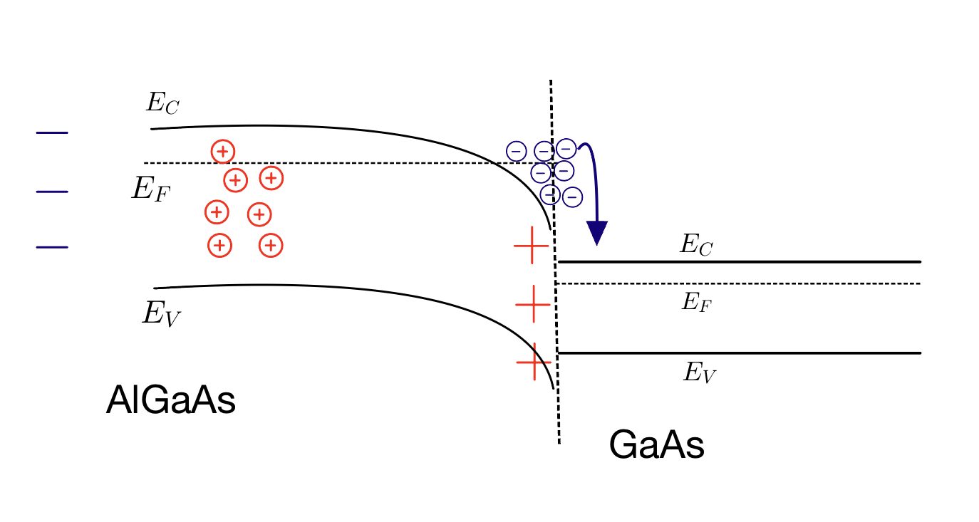
Figure adapted from Ref[3]
Next, consider that the material is now connected to GaAs, which has a smaller bandgap residing in the range of AlGaAs bandgap. Negative charges at the interface will find it more favourable to fill the lower energy state that is in the GaAs side of the heterostructure interface.
When the equilibrium is reached the quasi-fermi level is constant across the interface, and bands are bent around the interface. This causes some of the negative charge carriers to stay above the conduction band in the GaAs as the equilibrium Fermi level is higher than the conduction band energy in the GaAs for a certain distance. Therefore, creating a triangular well confined in the horizontal direction of these sketches (z-direction), where the trapped carriers are only allowed to move in the x-y plane, hence the two dimensions.
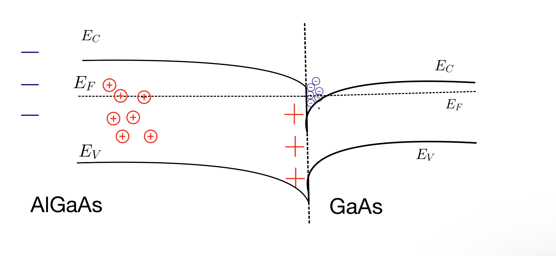
Figure adapted from Ref[3]
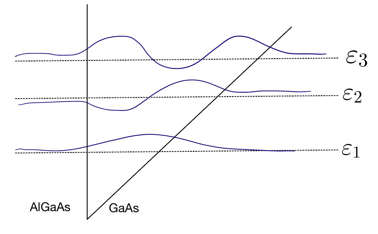
Figure adapted from Ref[4]
This length in the z-direction is so narrow that a significant level of quantisation is achieved, where different eigenvalues represent different subbands which would correspond to different density of states in the 2DEG. The subbands formed in the triangular quantum well are shown with a hand sketch. In our research, we are usually interested in accessing the lowest 2D subband during our experiments.
Transport in Low Dimensional Semiconductor Nanostructures on 2DEG
In a 2DEG electron motion is restricted to 2 dimensions, where the other dimension is about 10nm thick, and the level of this confinement does not allow for the electron wavefunctions to spread or move along the third dimension.
By applying voltage onto metallic gates, which could be placed on top of the semiconductor heterostructure, one can electrostatically define further confinement on the two-dimensional plane of 2DEG
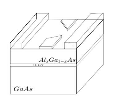
Sketch of the AlGaAs/GaAs heterostructure, with two metallic gates on top and large contacts at two ends
Quantum Point Contacts (QPCs) were one of the first confinement geometries realised on 2DEGs [5]. They were used to explore the electronic transport phenomena in low-dimensional systems and were one of the first devices to show quantisation of conductance as formalised by Landauer-Buttiker formalism [6][7]. For an ideal QPC under the ballistic regime, conductance is shown to be quantised with respect to the number of modes, M, contributing to the conduction:

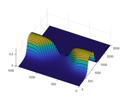
MATLAB simulation of the electrostatic confinement potential on the two-dimensional plane. It can be seen that the channel width (tunneling/channel probability) can be tuned by the applied potential from the gates.
This result was particularly interesting as the resistance is generally modelled as:

What happens when the length tends towards zero?
Need for Confinement
A thin conductor (1D) between two large contacts is a starting point to consider the conductance quantisation. In the conductor, the subbands are "countable", in contacts we observe a very large number of subbands which are not "countable" [1]. If the width of the conductor is less than the fermi wavelength and the length of the conductor is less than the mean free path of the charge carrier, the system is a ballistic one-dimensional transport system in which the subbands that contribute to the conductance are countable [8].

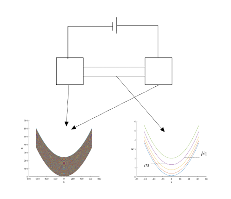
The chemical potential at the source and drain determines the number of subbands that are contributing to conductance where each of the subbands has a minimum energy above which the subband contributes. For a given energy, the number of transverse modes (or subbands contributing to the conductance) can be calculated as a function of excitation energy, E [1].

This is the M which multiplies the conductance quanta resulting in the expression of the conductance quantisation - the number of contributing subbands.
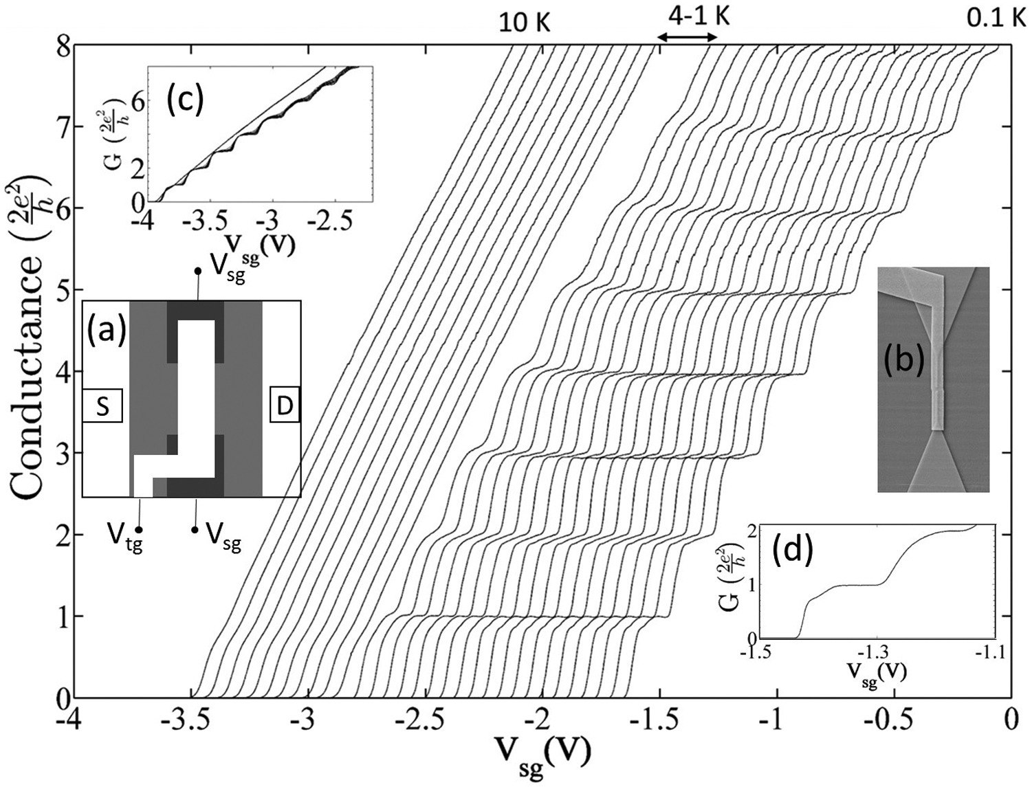
Cooldown characteristic and device layout of a typical one-dimensional (1D) quantum wire. (a) A schematic of the device consisting of a pair of split gates (in black), and over it, a cross-linked polymethyl methacrylate (PMMA) in grey acts as a dielectric for the top gate in white. S and D form the source and drain for the two terminal conductance measurements. (b) A magnified scanning electron micrograph of a top-gated, split gate device. The top gate spans an area of 1 μm, and the split gate is 400 nm long and 700 nm wide. (c) A conductance plot of a 1D device as the sample was cooling down in a dilution refrigerator. The starting temperature was 10 K and continuous split gate voltage sweeps were performed until the base temperature was 100 mK. The main plot shows the data in (c) replotted by setting a horizontal offset between the consecutive traces. On the top, a temperature range is indicated which is not true to scale. (d) A well-defined 0.7 conductance anomaly is observed at 100 mK in a different cooldown [9]. Figure taken from Ref[9].
Why so cold?
As can be seen above, the conductance plateaus that are in units of conductance quantum, disappear as the temperature increases. This is due to the temperature dependence of the Fermi-Dirac distributions

At finite temperatures, conductance can be expressed as a function of the above distribution, this was previously approximated as a step function [1].

Published experiments show the reproducibility of results; however, different temperatures yield different plateaus. Furthermore, it is shown that the geometry of the electrostatic confinement also affects the quantisation [10]. There is never a perfect quantisation under zero magnetic field; with a realistic geometry, the flatness of plateaus shows a 1% deviation. Moreover, the experimental results show that the best-quantised plateaus occur at finite temperatures [11].
Finally, a characteristic temperature exists for a ballistic system where thermal smearing dominates, and plateaus disappear. When the width of the thermal smearing is comparable to the Fermi level's subband spacing, we expect the plateaus' disappearance. This characteristic temperature could be expressed as follows [8]:

References
[1] S. Datta, Electronic Transport in Mesoscopic Systems (Cambridge University Press, Cambridge, 1995). [2] M. Kelly, Low-dimensional Semiconductors: Materials, Physics, Technology, Devices (Clarendon Press, Oxford, 1995). [3] H. Xiao-Guang et al., Formation of two-dimensional electron gas at AlGaN/GaN heterostructure and the derivation of its sheet density expression, Chin. Phys. B 24, 067301 (2015).[4] H. Bruus and K. Flensberg, Many-Body Quantum Theory in Condensed Matter Physics: An Introduction (Oxford University Press, Oxford, 2004). [5] B. Wees et al., Quantized conductance of point contacts in a two-dimensional electron gas, Phys. Rev. Lett. 60, 848 (1988). [6] R. Landauer, Spatial Variation of Currents and Fields Due to Localized Scatterers in Metallic Conduction, IBM J. Res. Dev. 1, 223 (1957). [7] M. Büttiker, Quantized transmission of a saddle-point constriction, Phys. Rev. B 41, 7906 (1990). [8] H. v. Houten, C. W. J. Beenakker and B. J. van Wees, Chapter 2: Quantum Point Contacts, Semiconduct. Semimet. 35, 9 (1992). [9] S. Kumar and M. Pepper, Chapter 2: Advances in interaction effects in the quasi one-dimensional electron gas, Semiconductor Nanodevices 20, 7 (2021). [10] H. Houten and C. Beenakker, Quantum Point Contacts, Phys. Today 49, 22 (1996). [11] B. Wees et al., Quantum ballistic and adiabatic electron transport studied with quantum point contacts, Phys. Rev. B 43, 12431 (1991).