Spintronics refers to the technologies which utilises the spin degree of freedom of the electrons in order to store or process information in addition to the charge.
Spintronic Technologies
In the 19th century, Lord Kelvin conducted the first experiments indicating that an applied magnetic field can change the resistance of a conductor [1]. Since then magnetoresistance has been a concept that is of interest in solid state and condensed matter physics. The discovery of Giant Magnetoresistance (GMR) and Tunnel Magnetoresistance (TMR) can be seen as the foundations of spintronics as a field of research and its use in today's technology [2][3][4]. TMR is an effect exploited in magnetic tunnel junctions, where a layer of insulator separates two ferromagnetic materials and the tunnelling between the layers can be controlled by the application of a magnetic field to each layer. If the magnetic orientation of the layers is parallel, tunnelling is easier and therefore there is lower resistance [4]. GMR is observed in various multilayer material structures which can combine non-ferromagnetic, anti-ferromagnetic or soft-ferro magnetic materials with ferromagnetic materials. It takes its name from the significant change in the resistance of these structures under an applied magnetic field [5]. Both of these effects are today exploited in technology and used in the development of new technologies such as:
Sensing (e.g, magnetic read-heads, biosensors)
Hard-Drives
Magnetic Random Access Memories
Furthermore, one can include how spin transport and detection are used in quantum computing approaches, alongside future spin-based memory and information processing technologies [6].
Semiconductor Based Spintronic Devices
Semiconductor-based spintronic devices, particularly spin-based field-effect transistors (spinFETs), hold the potential to revolutionise transistor technology by using electron spin degree-of-freedom in addition to charge. The attraction comes from its potential to develop devices faster and economically more efficiently [7].
The initial proposal for such a device was based on the idea of controlling electronic transport by applying an electric field to modulate the spin orientation of electrons moving between the source and drain [8].
These devices operate similarly to traditional transistors but this mechanism enables faster switching (turn-on/turn-off) times, potentially advantageous for information processing Furthermore, spin transport-based transistor systems can reduce the generated heat and allow for denser, various more energy-efficient information processing systems [7][9]. Current modulation in quasi-one-dimensional spin FETs and vertical spin MOSFETs have been reported [9][10].
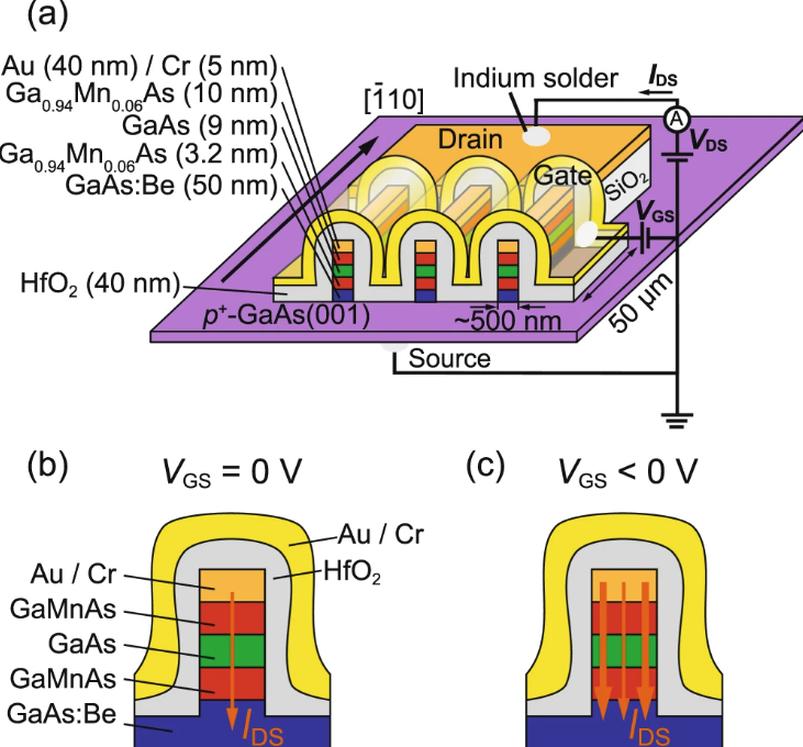
(a) Schematic illustration of the vertical spin MOSFET investigated in Ref[9]. The backside of the substrate is the source electrode, the comb-shaped Au/Cr layer is the drain electrode and the Au/Cr layer above the HfO2 layer is the gate electrode. (b,c) Schematic device operation of our vertical spin MOSFET when a gate voltage VGS is not applied (b) and when a negative gate voltage is applied (c). The orange arrows represent a drain-source current IDS. Figure taken from Ref[9]
Our investigation of transport phenomena in 2DEG at ultra-low temperatures where exotic behaviour and complex many-body effects are observed can bring new perspectives into spin-associated phenomena in nanostructures. Semicondcutor-based spintronic technologies are a recently flourishing field where fundamental research into such systems' dynamics is very exciting for us.
.
References
[1] W. Thomson, XIX. On the electro-dynamic qualities of metals:—Effects of magnetization on the electric conductivity of nickel and of iron, Proc. R. Soc. Lond. 8, 546 (1857).
[2] M. Baibich et al., Giant Magnetoresistance of (001)Fe/(001)Cr Magnetic Superlattices, Phys. Rev. Lett. 61, 2472 (1988).
[3] G. Binasch et al., Enhanced magnetoresistance in layered magnetic structures with antiferromagnetic interlayer exchange, Phys. Rev. B 39, 4828 (1989).
[4] M. Julliere, Tunneling between ferromagnetic films, Phys. Lett. A 54, 225 (1975).
[5] L. Chang et al., A brief introduction to giant magnetoresistance, arXiv:1412.7691 (2014).
[6] A. Hirohata et al., Review on spintronics: Principles and device applications, J. Magn. Magn. Mater. 509, 166711 (2020).
[7] R. Pela and L. Teles, Spin transistors vs. conventional transistors: what are the benefits?, J. Supercond. Nov. Magn. 23, 61 (2010).
[8] S. Datta and B. Das, Electronic analog of the electro‐optic modulator, Appl. Phys. Lett. 56, 665 (1990).
[9] T. Kanaki et al., Large current modulation and tunneling magnetoresistance change by a side-gate electric field in a GaMnAs-based vertical spin metal-oxide-semiconductor field-effect transistor, Sci. Rep. 8, 7195 (2018).
[10] P. Chuang et al., All-electric all-semiconductor spin field-effect transistors, Nat. Nanotechnol. 10, 35 (2015).